GoldenCZ
Mini/Micro-LED Technology Solutions
S-20ABFUD-T
GaN Blue LED Chip
Product Overview
| Model | Chip Material | Emitting Light | Package Type |
|---|---|---|---|
| S-20ABFUD-T | GaN | BLUE | Chip |
High Brightness, Long Lifespan
100% Chip Testing & Sorting
Excellent Wavelength Consistency
Mini LED Chip Technology
Low Power Consumption
Gold Electrodes
Applications
LED Filament
Optical Indicators
Indoor Displays
Smart Appliances
Package Dimensions
Chip Dimensions (20mil × 6mil)
Length
20 mil(508±38μm)
Width
6 mil(152±38μm)
Thickness
4.7 mil(120±15μm)
Electrode Specifications
P Electrode
GoldMaterial
N Electrode
GoldMaterial
Pad Dimensions
P Pad
4.5×6.3 mil(115±15×160±15μm)
N Pad
4.5×6.3 mil(115±15×160±15μm)
P-N Gap
5.9 mil(150±15μm)
Electrical & Optical Characteristics
At Ta = 22°C
| Parameter | Symbol | Test Conditions | Min. | Typ. | Max. | Units |
|---|---|---|---|---|---|---|
| Forward Voltage | Vf1 | If=5mA | 2.6 | - | 2.8 | V |
| Forward Voltage | Vf4 | If=1μA | 2.2 | - | 2.5 | V |
| Reverse Current | Ir | Vr=-7V | 0 | - | 1 | μA |
| Dominant Wavelength | λd | If=5mA | 445 | - | 462.5 | nm |
| Spectral Bandwidth | Δλ | If=5mA | - | 14.4 | - | nm |
| Radiant Flux A65 | PO A65 | If=5mA | 6.5 | - | 7.0 | mW |
| Radiant Flux A70 | PO A70 | If=5mA | 7.0 | - | 7.5 | mW |
| Radiant Flux A75 | PO A75 | If=5mA | 7.5 | - | 8.0 | mW |
Absolute Maximum Ratings
| Parameter | Symbol | Test Conditions | Rating | Units |
|---|---|---|---|---|
| Forward DC Current | If | Ta = 22°C | ≤30 | mA |
| Junction Temperature | Tj | - | ≤150 | °C |
| Storage (Chip) | Tstg | Chip | -40~+85 | °C |
| Storage (Tape) | Tstg | Chip-on-tape/storage | 0~40 | °C |
| Transport (Tape) | Tstg | Chip-on-tape/transport | -20~+65 | °C |
| Package Temperature | - | - | 280(<10s) | °C |
Performance Characteristics
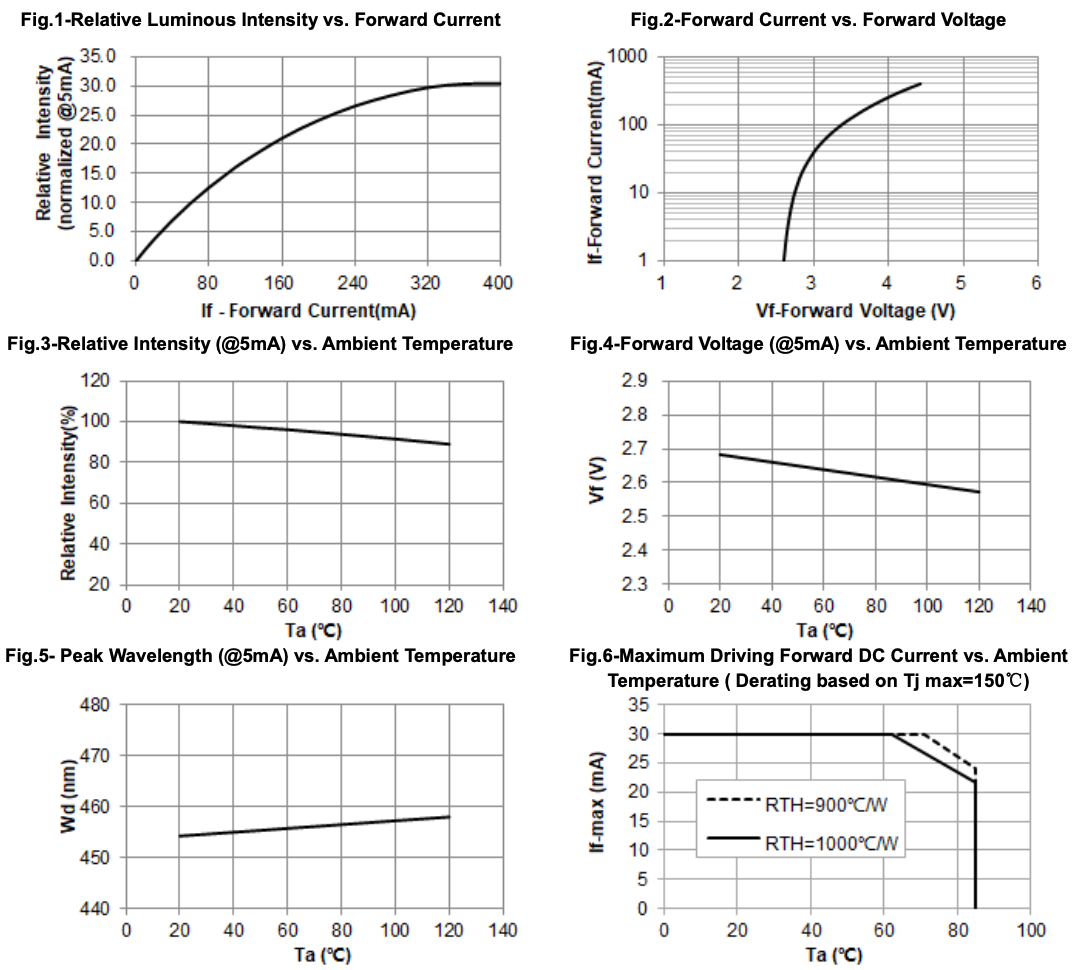
S-20ABFUD-T Performance Characteristic Curves
Performance Characteristics Summary:
• Fig.1: Relative Luminous Intensity vs. Forward Current
• Fig.2: Forward Current vs. Forward Voltage
• Fig.3: Relative Intensity (@5mA) vs. Ambient Temperature
• Fig.4: Forward Voltage (@5mA) vs. Ambient Temperature
• Fig.5: Peak Wavelength (@5mA) vs. Ambient Temperature
• Fig.6: Maximum Driving Forward DC Current vs. Ambient Temperature (Derating)
445-462.5nm
Wavelength Range
6.5-8.0mW
Radiant Flux
2.6-2.8V
Forward Voltage
≤30mA
Max Current
Important Operating Notes
• GaN LED chips are electrostatic sensitive devices - use ESD protection
• Wavelength span: 2.5nm, dominant wavelength measurement error: ±1.0nm
• Optical parameters tested under wafer conditions using testing equipment
• Radiant flux measurement error: ±10%
• Forward voltage measurement error: ±0.05V
• Maximum ratings defined under independent packaging conditions on PCB without encapsulation
• Store in controlled environment with proper humidity control
• Use current limiting to prevent overcurrent damage
Quality Assurance
100% electrical testing
Optical parameter verification
Wavelength sorting & binning
Reliability testing
Temperature cycling validation
ESD protection verification
Design Guidelines
Operating current: 5-30mA recommended
Operating temperature: -40°C to +85°C
Use current limiting circuits
Consider thermal management
Proper wire bonding to gold pads
ESD protection in handling