GoldenCZ
Mini/Micro-LED Technology Solutions
GFB0F19B
InGaN Green LED Chip
Product Overview
High Radiant Flux
High Current Intensity
Long Operation Life
InGaN Technology
Gold Alloy Electrodes
Temperature Stable
Applications
General Lighting
Digital Products
Display Backlighting
RGB LED Systems
Mechanical Specifications
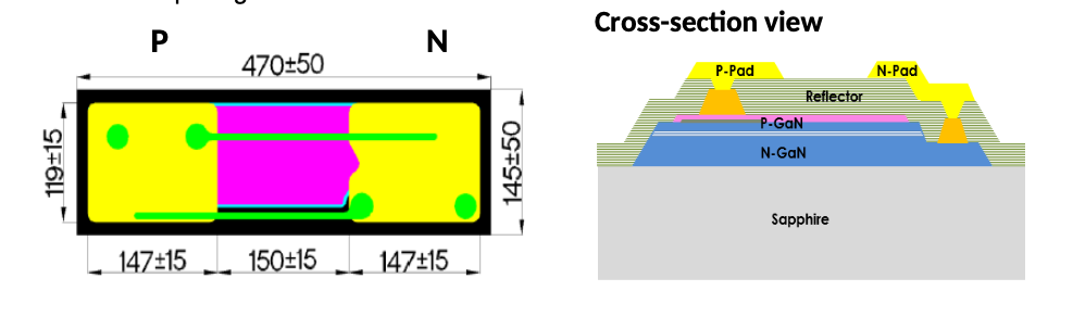
GFB0F19B LED Chip Diagram
Chip Size
145±25 × 470±25μm
Thickness
120±15μm
P Bonding Pad
119±15 × 147±15μm
N Bonding Pad
119±15 × 147±15μm
P-N Gap Distance
150±15μm
Electrode Material
Au AlloyP & N
Electro-Optical Characteristics
At Ta = 25°C
| Parameter | Symbol | Condition | Min. | Typ. | Max. | Unit |
|---|---|---|---|---|---|---|
| Forward Voltage | Vf | If=1μA | 2.0 | - | 2.2 | V |
| Forward Voltage | Vf | If=5mA | 2.3 | - | 2.6 | V |
| Reverse Current | Ir | Vr= -7V | 0 | - | 0.1 | μA |
| Radiant Flux | PO | If= 5mA | 4 | - | 5.6 | mW |
| Dominant Wavelength | Wd | If= 5mA | 517.5 | - | 532.5 | nm |
Absolute Maximum Ratings
| Parameter | Symbol | Condition | Rating | Unit |
|---|---|---|---|---|
| Forward DC Current | If | Ta=25℃ | ≤20 | mA |
| Reverse Voltage | Vz | Ta=25℃ | ≥ 7 | V |
| Reverse Current | Ir | Ta=25℃ | ≤1 | μA |
| Junction Temperature | Tj | - | ≤125 | ℃ |
| Package Temperature | - | - | 280 (<10s) | ℃ |
| Storage Temperature | - | Chip on tape | 0~40 | ℃ |
Characteristic Curves
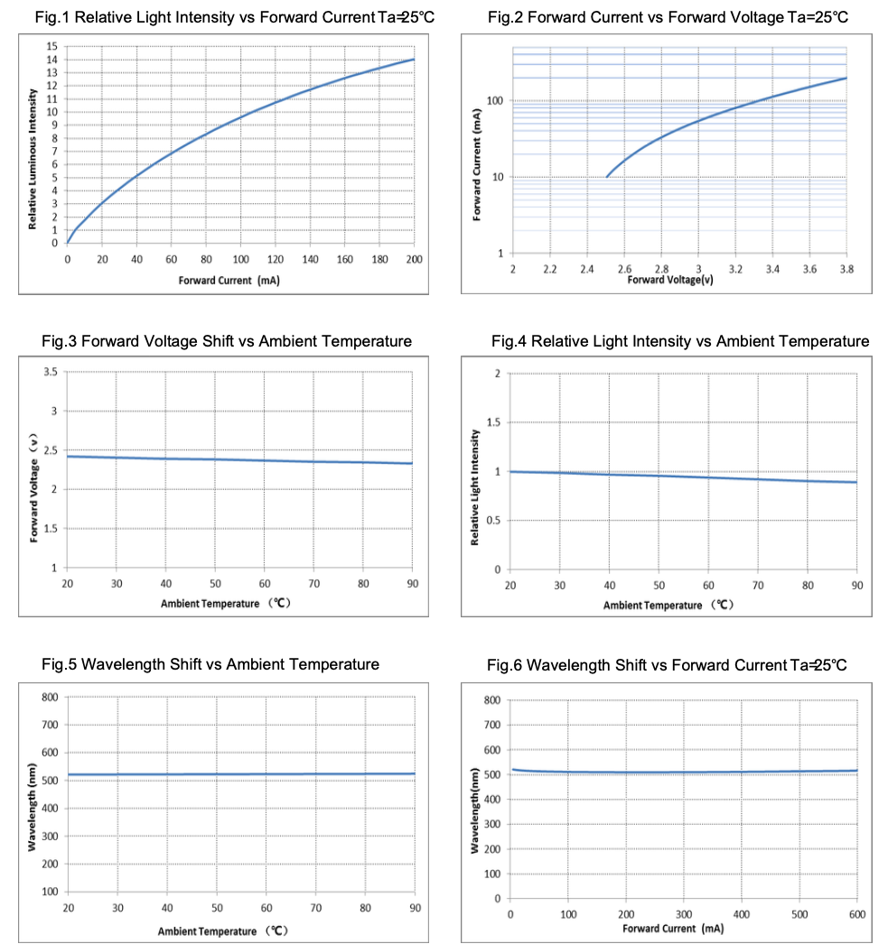
GFB0F19B Performance Characteristic Curves
517.5-532.5nm
Wavelength Range
4-5.6mW
Radiant Flux
2.3-2.6V
Forward Voltage
≤20mA
Max Current
Bin Definitions
| Items | Units | Bin1 | Bin2 | Bin3 | Bin4 | Bin5 | Bin6 |
|---|---|---|---|---|---|---|---|
| WD | nm | 517.5-520 | 520-522.5 | 522.5-525 | 525-527.5 | 527.5-530 | 530-532.5 |
| Lop | mW | 4-4.4 | 4.4-4.8 | 4.8-5.2 | 5.2-5.6 | - | - |
| VF | V | 2.3-2.4 | 2.4-2.5 | 2.5-2.6 | - | - | - |
| VF3 | V | 2.0-2.1 | 2.1-2.2 | - | - | - | - |
Packing Specification
Blue Tape Layout
Blue tape: (200±10) × (200±10) mm
Chip attachment area with organized layout
Label in lower-right corner
Complete tracking information
Label Contents
Company name and model
Date and quantity
Electro-optical parameters
Bin sorting information
Quality & Handling Guidelines
• All electro-optical characteristics tested with Golden CZ standard equipment
• Tolerance limits: Po ±6%, Wd ±1nm, VF ±0.06V
• ESD sensitive device - use proper anti-static precautions
• Store in controlled environment (0-40°C)
• Handle with care to avoid mechanical damage
• Use appropriate bonding techniques for Au alloy electrodes
• Recommended operating current: 5-20mA for optimal performance
Design Considerations
Select appropriate bin for color consistency
Account for temperature-dependent shifts
Use proper wire bonding techniques
Consider optical coupling efficiency
Implement current limiting circuits
Thermal management for high-power use